Image Processing
Accelerated by FPGAs
There is a considerable growth in the amount of data being generated by cameras particularly in the fields of quality inspection systems, public security and monitoring. With the increasing number of cameras, frame rates and resolutions even powerful back-end video processing systems are quickly reaching their limits. The approach to overcome this is to use a distributed computing platform, equipped with intelligent frame-grabbers which not only deliver a pre-filtering of the camera data but also make local decisions based on the input. This significantly reduces the data traffic to the backend system and fulfills deterministic real-time requirements.
Edge devices for vision processing and frame-grabbing can be composed of general and special purpose processors, FPGAs or any combination thereof. FPGAs offer advantages in pipelining and parallelism, which can be applied to most image processing operations. A general purpose CPU should be used for simple image processing tasks that require the use of software libraries. It is also useful for local system administration and setup. An architecture comprising of CPU and FPGA therefore offers a good balance in terms of flexibility cost and processing performance. The figure shows the dataflow of a frame grabber based on GigE-Vision.
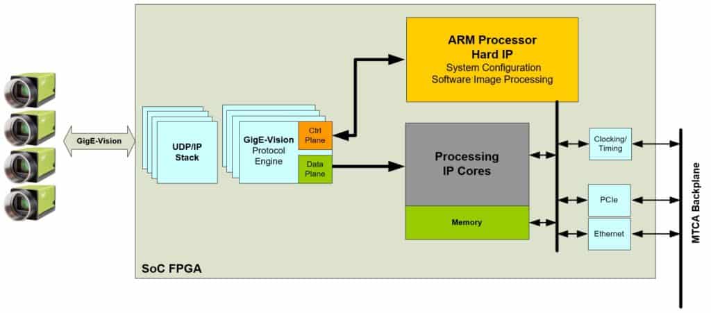
GigE-Vision is an Ethernet based open industrial transport protocol to connect cameras with cables up to 100m in length. Combined with Power-Over-Ethernet (PoE) the cameras can be connected with a single wire. The programmable logic part in the system is responsible for the image processing part and the termination of the GigE-Vision protocol to the front-end camera and transporting processed image data to the backend system.
The ARM processor performs administrative tasks by initializing the system to match the camera parameters. Since the processor shares its main memory with the FPGA, it can also actively participate in image processing. Usually these are lightweight tasks like dynamic labeling or scaling of image data. The combination of CPU and FPGA forms a very efficient and flexible platform which is able to process and terminate four camera streams in parallel.
FPGA Pixel Streaming
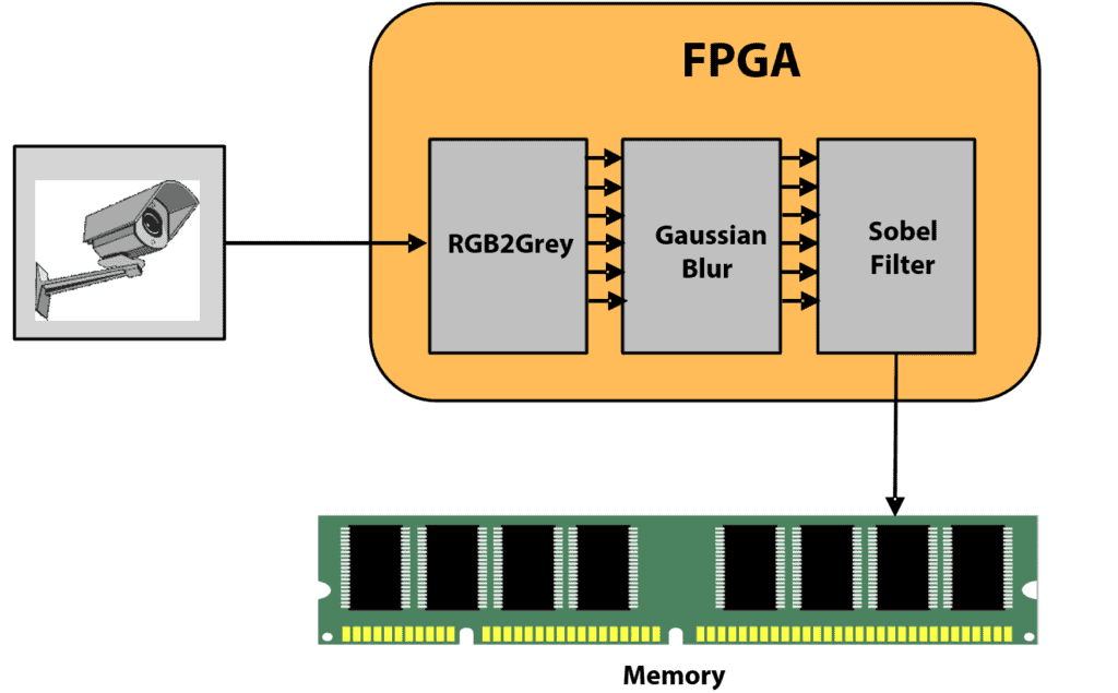
Pixel streaming is the way FPGAs process image data internally. Calculations are applied to individual pixels rather than processing whole frames at once. Traditional video processing platforms require many memory accesses, typically one per processing step. For example, the application of an edge detection filter requires at least four memory accesses, as shown in the image below. An FPGA manages with only one memory access, which has an advantage for system latency and thus frame rate.
FPGA Parallelization
The nature of FPGAs is to perform parallel processing. Applying this to image processing, the latency on pixel streams can be significantly reduced. The following diagram shows that the overall latency of a Sobel Filter algorithm decreases from 7.5 to 1.7 nanoseconds by using a parallelization factor of 8 pixels per clock cycle. Generally there is no limit in parallelization considering limitations of available image processing libraries.

FPGA Pipelining
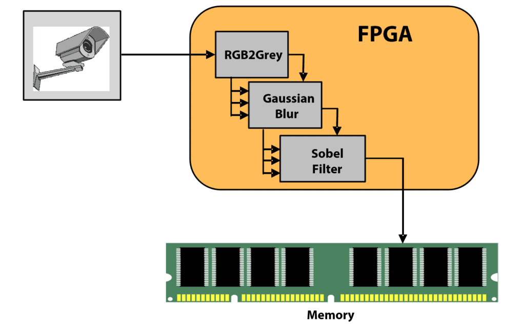
Additionally, pixel streaming can take advantage of decoupling signal processing stages by using the pipeline approach. With pixel pipelining the processing stages are interleaved allowing the next stage to start before the previous has completed its operation. This technique furthermore reduces the latency and improves the overall performance.
Performance analysis among different platforms
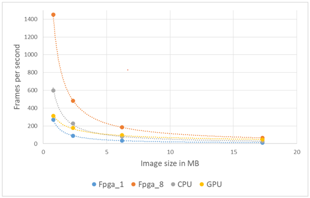
The following figure shows a comparison among common image processing platforms calculating a Sobel Edge Detection image filter. For the comparison we have used mid-range devices in each class using similar libraries based on OpenCV. Especially when it comes to small image sizes the FPGA is much more efficient than the other devices. It is also noticeable that the parallel computing of eight pixels per clock cycle linearly scales the data throughput inside the FPGA. Small image sizes require the CPU and GPU to do many memory transactions which adds a lot of latency to the overall processing pipe. This leads to the effect that these devices cannot develop their full efficiency. FPGA devices do not show this effect.
Platform | Library | Tool | Image Filter | ||
|---|---|---|---|---|---|
Nvidia Geforce GTX 1050 | OpenCV with CUDA | MS Visual Studio | Sobel Edge Detection | ||
Intel i7 8700 @ 4.6 GHz | OpenCV | MS Visual Studio | Sobel Edge Detection | ||
Xilinx ZYNQ-7020 | xf-OpenCV | Vivado + Vivado HLS | Sobel Edge Detection | ||

Contents of a FPGA video processing design
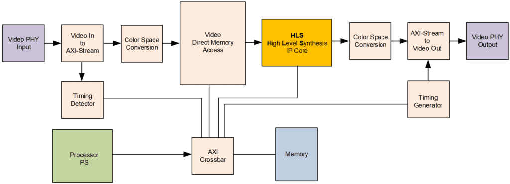
Vendors of FPGA devices (Xilinx, IntelFPGA) offer built in IP cores to setup the vision processing infrastructure as shown in the figure below. Basically the FPGA design needs to implement a path to convert the input data stream from the camera into a streaming format, such as AXI-Stream and vice versa to the output device. As a function of the FPGA one can adapt easily to any camera I/O standard such as GigE-Vision and HDMI. Timing information of native video signals contain the resolution and frequency of the image. Timing signals are required when it comes to storage and buffering of images in memories. Buffering is usually done by a video DMA block which plays a central role to reduce backpressure in the processing chain thus untighten input and output data streams. The ARM processor is AXI memory mapped connected with the processing chain to setup up and control the data stream. It would also be possible to perform lightweight calculations on the image stream based on high level software libraries, such as OpenCV.
Acceleration with High Level Synthesis (HLS)
HLS is used to describe FPGA algorithms using a C programming language. In many situations in image processing this is a clear advantage, because most algorithms are based on loops. Furthermore, proven image processing libraries available in C can be used as support. The functional principle of HLS is based on an HLS compiler, which transfers the C code into an HDL circuit and exports it as IP core if necessary. In doing so, the loops are rolled out and the content is processed in parallel. The resulting performance can be up to a hundred times faster than what it takes to run a similar algorithm on a CPU. In addition, algorithms developed with HLS can be simulated and tested much more easierbecause the module is called as a C function in a C program test environment.
- Describe FPGA algorithms with a C language (C or C++)
- Use available image processing libaries as support
- Compile C code into HDL logic with the HLS compiler
- Archive up to 100+ performance gain
- Test and simulate your module as C program
- Export algorithm as HDL IP-Core if necessary


